|
|
|
|
|
上海交通大学、武汉大学两位专家讲述三维封装集成技术 |
|
|
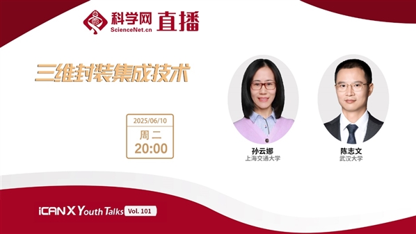
直播时间:2025年6月10日(周二)20:00-21:30
直播平台:

科学网APP
https://weibo.com/l/wblive/p/show/1022:2321325175995988050033
(科学网微博直播间链接)

科学网微博

科学网视频号
北京时间6月10日晚八点,iCANX Youth Talks第101期邀请到了上海交通大学副研究员孙云娜、武汉大学副教授陈志文担任主讲嘉宾,太原理工大学副教授郭星、南洋理工大学博士后研究员李亚辉担任研讨嘉宾,上海交通大学教授杨卓青担任主持人,期待你一起加入这场知识盛宴。
【嘉宾介绍】
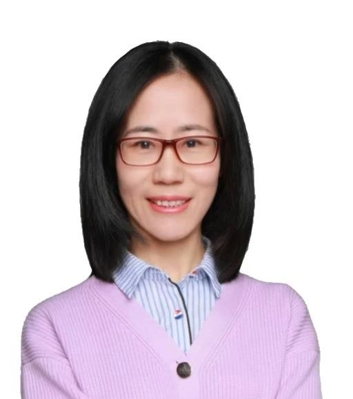
孙云娜
上海交通大学
高密度电子系统的热管理技术演进:从三维异构集成到热流调控
【Abstract】
Thermal management in high-density electronic systems has emerged as a critical challenge constraining the energy efficiency and reliability of information devices. The advancement of 3D heterogeneous integration technology has driven heat flux density beyond 1 kW/cm², while the improvement in heat dissipation capacity of traditional thermal management solutions is insufficient. This report systematically presents technological breakthroughs from fundamental thermophysics principles to multiphysics-field collaborative regulation: 1) Solid transfer thermal resistance: By leveraging high-thermal-conductivity material systems, optimizing size, and implementing structural enhancements, thermal resistance is effectively diminished. 2) Thermal diffusion resistance: Utilizing heat source topological reconstruction and optimizing hot-wire array layouts, heat diffusion efficiency is significantly bolstered. 3) Interfacial thermal resistance: By strengthening material interfacial layers and effectively expanding the thermal resistance reduction, interfacial thermal resistance is notably reduced. 4) Convective heat transfer resistance: By designing bio-inspired microchannel structures and adopting jet-duct coupling designs, boundary layers are compressed, fluid flow states are regulated, fluid flow characteristics are enhanced, and the convective heat transfer area is substantially increased. These research findings provide a solid theoretical foundation for the thermal design of high-performance computing chips and chiplets, and contribute to the advancement of thermal management technology for high-density electronic systems.
高密度电子系统的热管理已成为制约信息器件能效与可靠性的核心挑战。三维异构集成技术推动芯片级热流密度突破1 kW/cm²,而传统热管理方案的散热能力提升幅度不足。本报告系统阐述从传热学基本原理到多物理场协同调控的技术突破:在固体传热热阻方面,从高热导率材料体系、尺寸和结构化降低热阻;在固体扩散热阻优化中,运用热源拓扑重构和热线阵列排布优化技术提升热扩散效率;在界面热阻领域,通过强化材料界面层、有效扩展热阻降低界面热阻;在对流换热热阻控制方面,设计仿生微通道结构实现边界层压缩、流体流态调控及对流换热面积的显著增加,采用射流-导流耦合设计强化化流体流动特性。这些研究成果为高性能计算芯片和芯粒的热设计提供了坚实的理论基础,有助于推动高密度电子系统热管理技术的进步。
【BIOGRAPHY】
Sun Yunna, Associate Professor at Shanghai Jiao Tong University. Her research focuses on microfluidic cooling technology, chiplet packaging technology and thermal-mechanical reliability, and MEMS microfabrication technology. She has led over 10 national/provincial key projects, including those supported by the Ministry of Education, pre-research key projects, National Natural Science Foundation, and national key laboratory funds. She has published over 70 papers (including 20 in top-tier journals such as Advanced Materials) and hold 15 authorized invention patents. Her research MECMP was awarded the "Special Prize for University Exhibition Area" at the 20th International Industry Fair.
孙云娜,上海交通大学副研究员,博士生导师。主要从事微流体散热技术、芯粒封装技术与热机械可靠性、MEMS微加工技术等方向的研究。主持国家级/省部级重点项目10余项,包括:教育部支撑重点项目、预研重点项目、国家自然科学基金项目、国家级重点实验室基金项目等。发表论文70余篇(含Advanced Materials等TOP期刊20篇),获授权发明专利15项。研发的多元兼容集成技术获第二十届国际工博会“高校展区特等奖”。
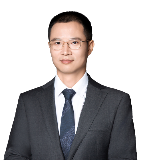
陈志文
武汉大学
先进封装互连技术
【ABSTRACT】
For a long time, semiconductor manufacturing technology has continuously advanced along Moores Law. In recent years, it has gradually approached physical limits, making advanced packaging increasingly critical for improving chip performance. To meet users ongoing pursuit of miniaturization and high performance, the industry has successively developed advanced packaging technologies such as Flip Chip, WLCSP (Wafer Level Chip Scale Packaging), Fan Out, 2.5D, and 3D packaging, with continuously improved packaging integration. Meanwhile, corresponding interconnection technologies have also evolved to meet the electrical, thermal, mechanical, and reliability requirements, which places higher demands on packaging design, processes, and reliability.This report systematically elucidates the characteristics of mainstream advanced packaging and corresponding interconnection technologies, focusing on a series of structural, material, and other changes brought about by the continuous miniaturization and innovation of interconnection bump scales. It emphatically expounds the impact of intermetallic compounds on reliability in micron-scale interconnection bumps and introduces the evolving interpretation of the mechanical properties of interconnection bumps.
长期以来半导体制造技术沿着摩尔定律不断发展,近些年已逐渐逼近物理极限,先进封装对于提升芯片性能的重要性日益凸显。为满足用户对于小型化和高性能的持续追求,业内先后发展出Flip Chip, WLCSP, Fan Out, 2.5D 及3D封装等先进封装技术,封装集成度不断提升。同时,相应的互连技术也不断演进,以满足相应的电学、热学、力学及可靠性需求,这对封装设计、工艺及可靠性等提出了更高的要求。本报告系统地梳理了主流先进封装的特征及相应互连技术,聚焦随着互连凸点尺度持续缩小和不断创新,带来一系列结构、材料等多方面的变化。着重阐述了微米尺度互连凸点中金属间化合物对可靠性的影响,介绍了业界对于互连凸点力学特性认识的不断深入和演变过程。
【BIOGRAPHY】
CHEN Zhiwen is an Associate Professor at Wuhan University. He is a recipient of the Hubei Provincial Outstanding Young Scientist Fund, and the Deputy Director of the Hubei Provincial Key Laboratory of Electronic Manufacturing and Packaging Integration. His research focuses on advanced packaging, interconnection technology, and multiscale simulation. In the field of advanced packaging, Dr. Chen has developed multiscale deformation characterization methods and multi-field ultrafast in-situ monitoring technologies with nanosecond-level time resolution. The key parameters have reached internationally leading level. He has elucidated the mechanisms of evolutions in microstructure and mechanical property at interconnection interfaces. Their effects on interconnection reliability have also been revealed. These works have provided technical supports to leading enterprises in addressing critical reliability challenges. High-performance ternary coatings have been developed to mitigate interface defects. And packaging stress regulation strategies were also proposed to significantly enhance the reliability of representative devices. His work has been published in journals such as Nature Communications, Materials Science and Engineering: A, and Journal of Alloys and Compounds. He has received honors including the National Defense Science and Technology Progress Award and the Outstanding Paper Award at the ICEPT Conference.
陈志文,武汉大学副教授,湖北省杰出青年基金获得者、电子制造与封装集成湖北省重点实验室副主任。研究领域:先进封装、互连技术、多尺度仿真。陈志文围绕先进封装领域研发多尺度变形表征方法和多场超快原位监测技术,时间分辨能力为纳秒级,达到国际领先水平;揭示互连界面微观组织生长行为和力学特性变化对可靠性影响规律,助力领军企业攻克可靠性难题;研发高性能三元镀层减少互连界面缺陷,提出封装应力调控方法,使典型器件可靠性指标显著提升。相关研究成果发表在Nature Communications,Materials Science and Engineering: A,Journal of Alloys and Compounds等期刊,获国防科技进步奖、ICEPT大会杰出论文奖等奖项。
【主持人】
杨卓青
上海交通大学
【研讨嘉宾】

郭星
太原理工大学

李亚辉
南洋理工大学
特别声明:本文转载仅仅是出于传播信息的需要,并不意味着代表本网站观点或证实其内容的真实性;如其他媒体、网站或个人从本网站转载使用,须保留本网站注明的“来源”,并自负版权等法律责任;作者如果不希望被转载或者联系转载稿费等事宜,请与我们接洽。